WCM Go to Chinese page Go to Japanese page Go to Korean page Go to German page Go to French page Go to Italian page     
Wafer Charging Monitors, Inc.


New from WCM!

Auto ChargeMap®
EOS/ESD Symposium News
GMR Fab Support

About WCM

Products and Services
Frequently Asked Questions
Vendor Presentations
Sales Representatives

Literature

Applications Tutorial
Latest Research!
Technical Notes & Briefs
Publications
Search (Abstracts)

Newsletter

Free Subscription Form
Current Issue
Archives


  The leading supplier of products and services for quantifying wafer charging in semiconductor process equipment including: ion implanters, ashers, etchers, and plasma deposition systems.  
wafer 
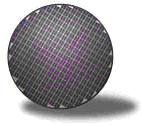
Charm®-2 Monitor Wafers
200, 150, 125, 100, and 75-mm
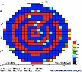
ChargeMap® Software
& Evaluation Services
chargemap


Wafer Charging Monitors, Inc.
127 Marine Road
Woodside, CA 94062
U.S.A.

tel: (650) 851-9313 . . . . fax: (650) 851-2252


Copyright © 1997-2015 Wafer Charging Monitors, Inc.
All rights reserved.
Last Modified: Feb. 10, 2015


wafer charging, charge monitor, charging damage, CHARM, charm, CHARM wafers, CHARM monitors, charging damage, process-induced damage, plasma damage, implant damage, UV damage, hi-current implant, oxide damage, plasma potential, plasma probe, SPIDER wafers, Quantox, SDI, Semiconductor Diagnostics, asher, downstream stripper, ion implanter, flood gun, E-shower, plasma etcher, resist stripper, semiconductor equipment, arsenic implant, ECR etching, gate etch, oxide etch, plasma deposition, plasma etch, plasma etching, polysilicon etch, sputter clean, via etch, gate oxide, thin oxides, IC reliability, in-line monitor, integrated circuits, wafer processing, yield improvement, wcm